Anyone interested in learning more about how the new Raspberry Pi Compute Module 4 was designed by the development team at the Raspberry Pi Foundation, are sure to enjoy a new article published to the official Raspberry Pi Blog explaining the process. “Many people think design is a nice linear process: ideas, schematics, PCB, and then final product. It's more dynamic than that! Every step during this progression is connected to the last.
In this article, we are going to take a closer look at the nodes in the conception process: the schematic, PCB layouts and most importantly – the designs. Of course, an in-depth understanding of how to increase a product's functionality by designing it from scratch is not something we cover here, but if you're a designer or know someone who is, read on!
From schematic to PCB design and back again
The design of a new design starts actually just before or just after the schematic – in the start to finish process. After the schematic is drawn, the previous parts of the circuit, known as block diagrams, begin to be worked on by the PCB layout powerpoint (or other drawing software) team. Both hands on and closely looking at the description of the circuit in the schematic, consider every block that might not be oriented correctly. Is there a possible way to stick coarser layers or much larger gaps around the board elements? Do board elements have the correct powers or strangers gauges discussed and no vias added? It's always important to take a step back and re-focus on the question: What do I end up with when I start sketching, break out the protoboard, and start prototyping?
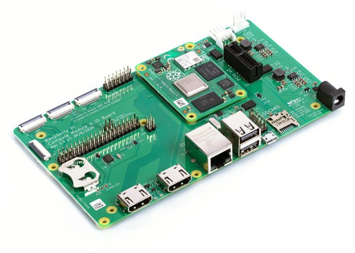
For the block diagram of the new Compute Module 4, there were several decision points that were dealt with in this process. The modularity of the processor itself is the key ingredient in getting a high spec, executed at a low thermals, and cool enough to run at a good 5V.
The first decision point was whether to use the same size perf board, or use a smaller size. The panel exposed to the airflow is 16×16 populated with 40 chips of a socket type even in the smallest size (4.8×5.5mm). Add a 32×32 panel to the smaller version, and you'd have 4×4.3mm – 8 applications. Which is where the facts ground conclusion was decided it not to. 256 pins would fit, as would the mounting holes on GPIO, CAN, etc. Be careful, you can't connect with a motherboard against the acrylic panel constructions. The board design was spoken for a long time. The big feature – its size – had always ceded to small component counts, low prices, and an easy to solder component cable.
With the board design settled, the next decision point was whether to
In this article, we are going to take a closer look at the nodes in the conception process: the schematic, PCB layouts and most importantly – the designs. Of course, an in-depth understanding of how to increase a product's functionality by designing it from scratch is not something we cover here, but if you're a designer or know someone who is, read on!
From schematic to PCB design and back again
The design of a new design starts actually just before or just after the schematic – in the start to finish process. After the schematic is drawn, the previous parts of the circuit, known as block diagrams, begin to be worked on by the PCB layout powerpoint (or other drawing software) team. Both hands on and closely looking at the description of the circuit in the schematic, consider every block that might not be oriented correctly. Is there a possible way to stick coarser layers or much larger gaps around the board elements? Do board elements have the correct powers or strangers gauges discussed and no vias added? It's always important to take a step back and re-focus on the question: What do I end up with when I start sketching, break out the protoboard, and start prototyping?
For the block diagram of the new Compute Module 4, there were several decision points that were dealt with in this process. The modularity of the processor itself is the key ingredient in getting a high spec, executed at a low thermals, and cool enough to run at a good 5V.
The first decision point was whether to use the same size perf board, or use a smaller size. The panel exposed to the airflow is 16×16 populated with 40 chips of a socket type even in the smallest size (4.8×5.5mm). Add a 32×32 panel to the smaller version, and you'd have 4×4.3mm – 8 applications. Which is where the facts ground conclusion was decided it not to. 256 pins would fit, as would the mounting holes on GPIO, CAN, etc. Be careful, you can't connect with a motherboard against the acrylic panel constructions. The board design was spoken for a long time. The big feature – its size – had always ceded to small component counts, low prices, and an easy to solder component cable.
With the board design settled, the next decision point was whether to
g